

For this DIY adventure, we’re going to be walking through the steps of building the Classic Delay pedal from Build Your Own Clone (BYOC), a company that has been a big player in the pedal-kit game for quite a while. This is a little more complicated than building a fuzz or overdrive, so I’m going to explain the process with great detail. Let’s get started.
Tools You’ll Need for This Project
- Soldering Iron
- Solder
- #2 Phillips screwdriver
- Wire strippers
- 8 mm (5/16") nut driver/wrench
- 10 mm (25/64") nut driver/wrench
- 1/2" nut driver/wrench
- 14 mm (9/16") wrench
- Flush cutters
- Small needle-nosed pliers
- Third hands
These tools are available via a variety of suppliers, including StewMac, Allparts, and Amazon.
Step 1: Review the Instructions
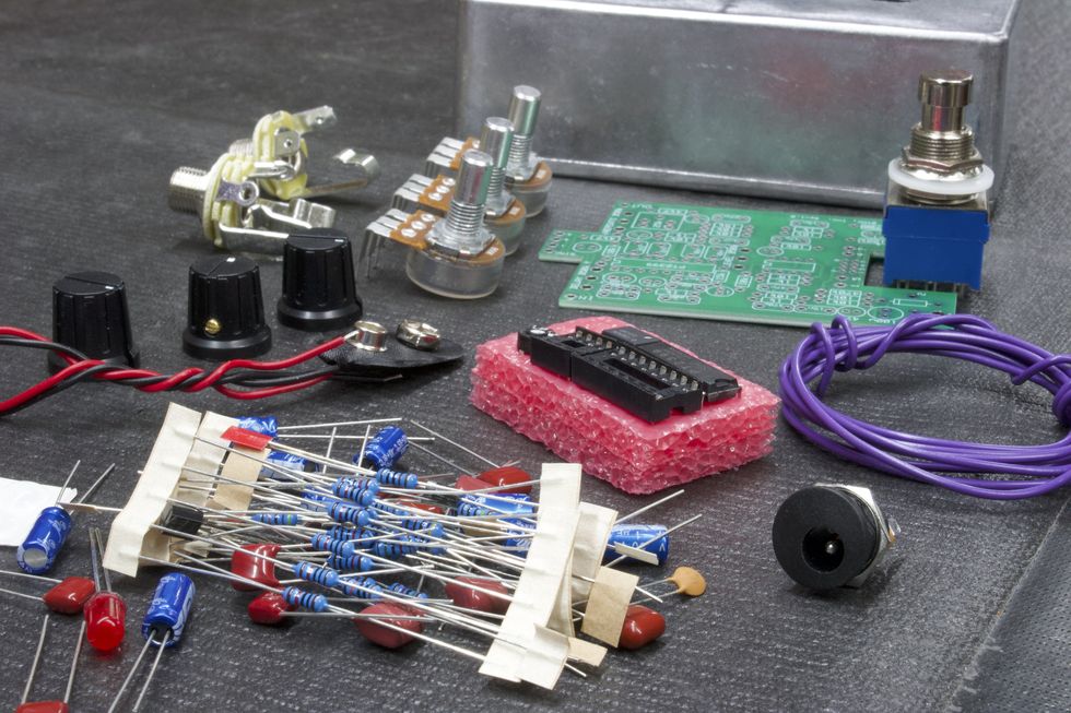
The kit as it arrives (Photo 2).
Each BYOC kit comes with a detailed set of instructions in the form of a PDF that can easily be printed out. The Classic Delay’s instructions can be found at https://www.byocelectronics.com/classicdelayinstructions.pdf. They are 32 pages long, and I suggest following their steps as you read this article. Here, I will refer to specific page numbers that correspond with the steps. I’ve also taken photos to coincide with the steps. Within the instructions, we find a table of contents, pictures of the fully assembled pedal, a list of parts included, and step-by-step instructions from internal population and soldering to external assembly. With any kit, always read the instructions carefully before you start building.
Step 2: PCB set-up
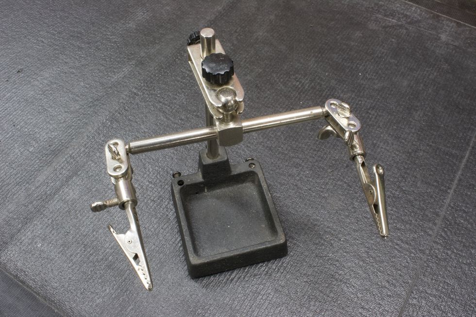
Photo 3
A lot of pedal builders use PCB jigs that are specifically designed to hold several printed circuit boards so that they can be easily populated and soldered. These jigs are great tools. However, they’re not something a casual DIY enthusiast will often have. Essentially, all we really need to do is elevate the PCB off of the working surface so that the leads of the components can pass through the bottom side of the PCB. This is most helpful with components that can be soldered from the top side of the PCB. “Third hands” or “helping hands” (Photo 3) are a good tool for this job. So, what can we do to elevate the PCB if we don’t have access to third hands? Simply turn the enclosure upside down and place the PCB perpendicular (Photo 4). This will elevate the PCB enough to allow the component leads to easily pass through.
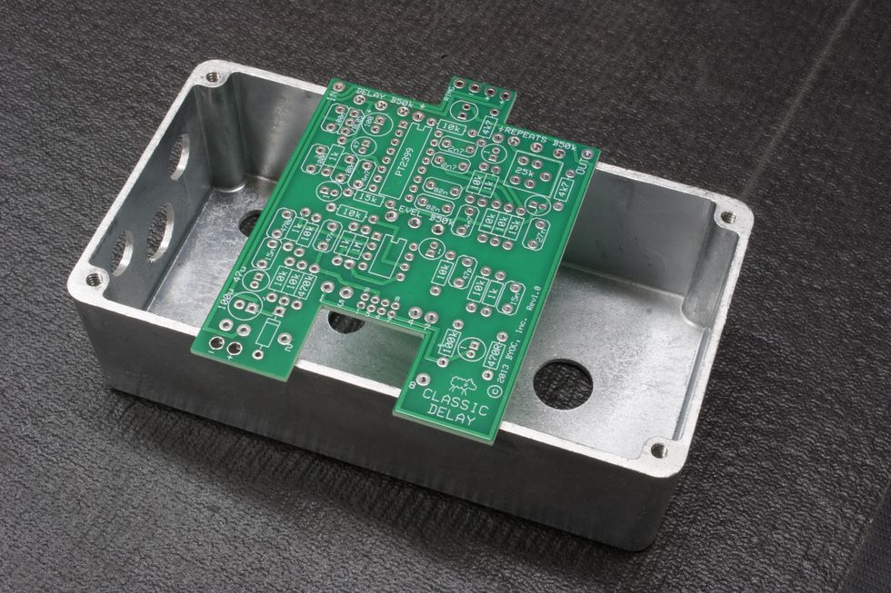
Photo 4
Step 3: Populating Resistors and Diodes (instructions page 9)
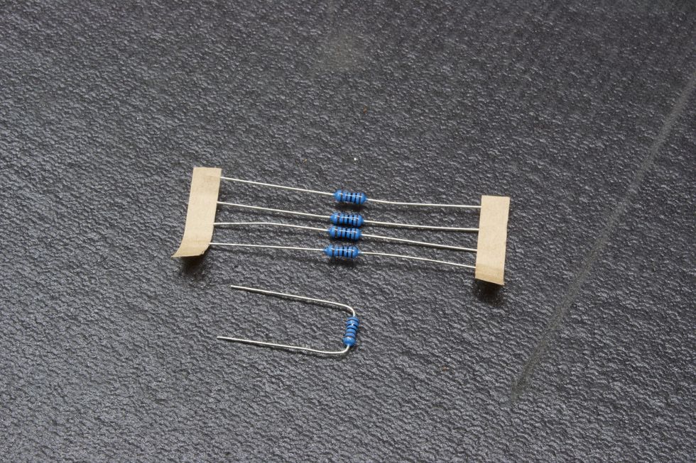
Photo 5
When populating PC boards, we typically like to work lowest to tallest in regards to the seating. Seating is how far above the PC board the component rests. Resistors and diodes sit pretty low to the PC board, so populating them first makes sense.
Resistors: Remove the resistor from the paper ribbon, bend the leads (Photo 5), and place them through the corresponding pads (Photo 6) as directed. (A pad, by the way, is the term for the designated surface area of a component’s electric contact point.) A good practice is to populate all resistors of the same value before moving on to the next value. Populate all 1k resistors, then all 10k resistors, and so on.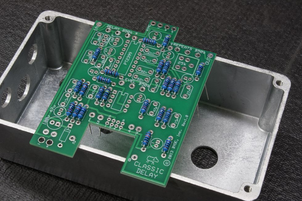
Photo 6
Reading resistor color bands can be confusing, so don’t forget the reference guide on page 7 of the instructions. Here, you will find a detailed breakdown of each value and its corresponding 5-band reading (i.e. 1k = brown/black/black/brown/brown). Once all the resistors are placed, we can go on to the diode.
Diode: Next, we need to place the diode. Just like resistors, remove the diode from the paper ribbon, bend the leads, and place them through the corresponding pads. Diodes are polarized and need to be oriented a certain way (Photo 7). Be sure to match the diode to the outline on the PCB, as shown on page 10 of the instructions.
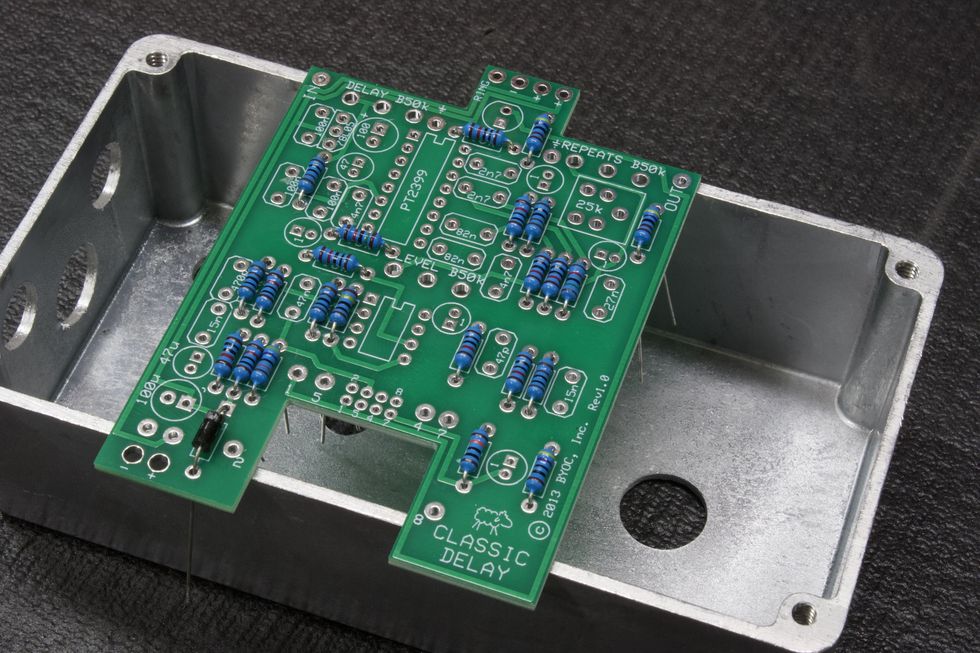
Photo 7
Step 4: Solder Resistors and Diode
Photo 8
Fire up the soldering iron! Once the iron is up to temperature (650 to 750 degrees Fahrenheit, depending on how fast you work), it’s time to get to work. Resistors and diodes can easily be soldered from the top side. So no need to flip the PCB over. Place the solder tip to the pad and feed the end of the tip a bit of solder. What we’re looking for here is solder that covers the entire pad, encapsulates the lead, and has a nice shine to it. Think of it like a shiny Hershey's Kiss shape (Photo 8). Repeat this step for every part. If you’re new to soldering, you should consult our concise guide to soldering, online or in PG’s October 2015 issue.
Soldering tip: Shut the iron off between population steps. Use a small, tabletop fan to blow the solder fumes away during soldering steps. Quick tutorial videos on YouTube are also of benefit here, for builders new to soldering.
Step 5: Trim the Leads
Photo 9
Next, place the PCB upside down to expose the leads (Photo 9). Using flush cutters, trim the excess leads (Photo 10).
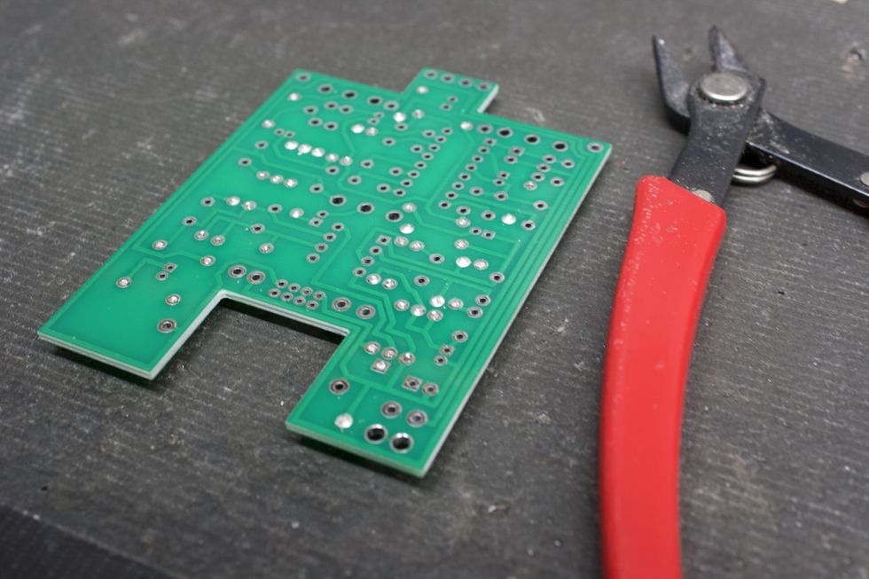
Photo 10
Step 6: Soldering IC Sockets (page 11)
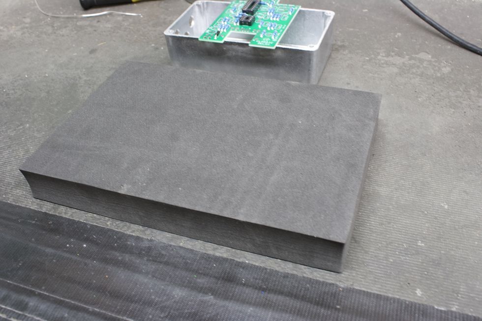
Photo 11
Place the 8-pin and 16-pin IC sockets into the corresponding pads on the top side of the PCB. We need to solder the IC socket pins from the bottom side. This means flipping the PCB over without having the IC sockets fall out. For this, I like to use a small piece of foam (Photo 11).
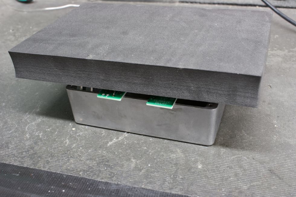
Photo 12
I place the foam on top of the PCB (Photo 12), then flip the foam and PCB simultaneously so the foam is below the PCB and the bottom side of the PCB is facing up (Photo 13).
Photo 13
For this soldering step, we’ll want to solder ONLY 1 pad and then flip the board over to ensure that the IC sockets are sitting flush. If the IC sockets are not flush, go back to the bottom side and reflow that solder pad while pressing the PCB downward and keeping it parallel to the work surface. Solder the remaining pads (Photo 14).
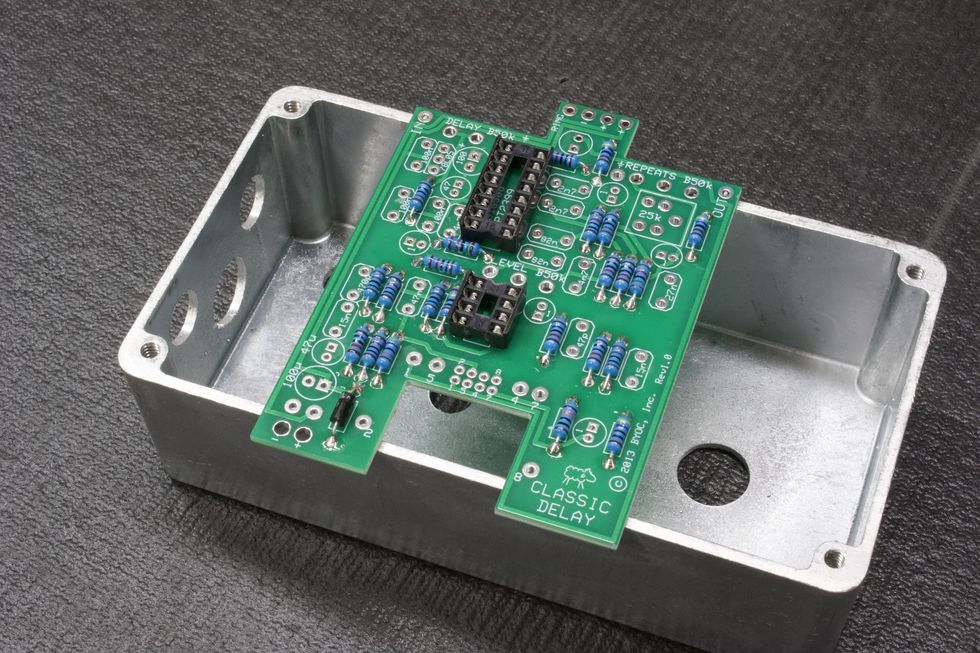
Photo 14
Step 7: Soldering the Voltage Regulator (page 12)
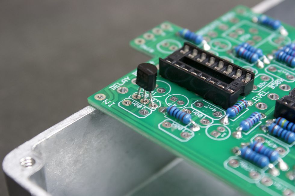
Photo 15
Place the voltage regulator into the three corresponding pads, while keeping mindful of the orientation. The flat side needs to match the outline on the PCB. Now, we’re ready to solder. This can be done from either side. Flush-cut the excess lead and we’re done here (Photo 15).
Step 8: Soldering the Trim Pot (page 13)
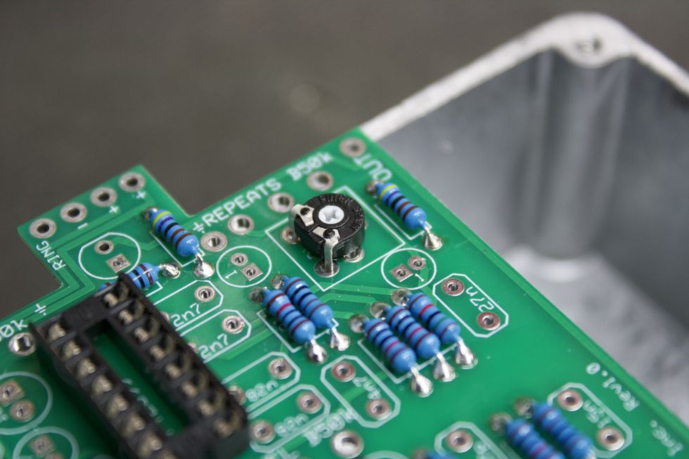
Photo 16
Place the trim pot (Photo 16) into its corresponding pads. For the trim pot provided, I found it easiest to solder the two exposed legs from the top side (Photo 17) and then the remaining leg from the bottom side.
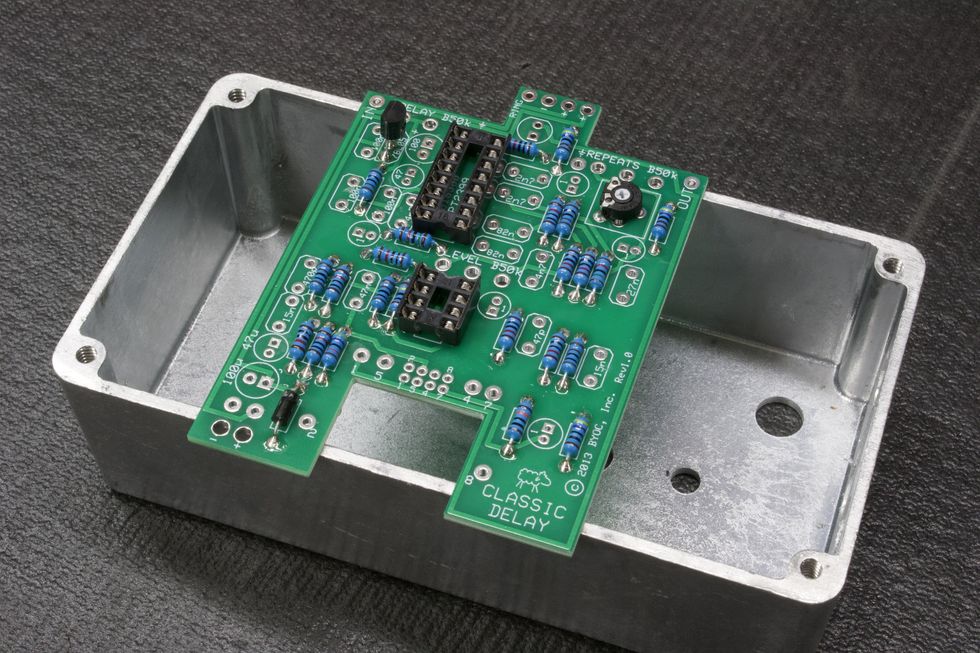
Photo 17
Step 9: Soldering Ceramic and Film Caps (page 14)
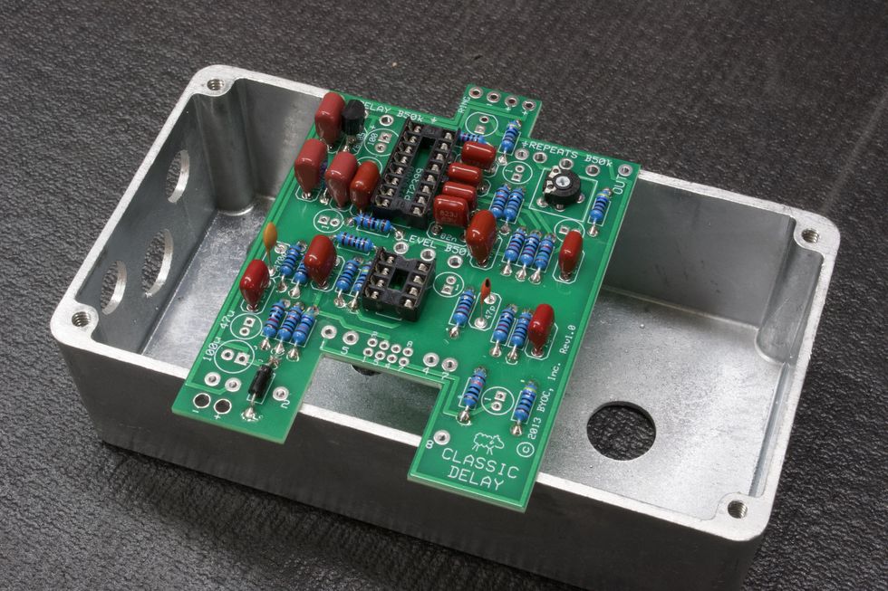
Photo 18
Place all ceramic (pill-shaped) and film (red) caps into their respective locations. Again, use page 7 of the instructions as a reference for identifying the correct capacitors (i.e. 100n film cap, which may say “104” or “.1” or “u1” on the body). We’ll need to solder the pads from the bottom side. So, once again, the piece-of-foam trick can be your friend here. Flush-cut the excess lead and we’re done (Photo 18).
Tip: An alternate method would be to bend the leads away from each other so they stay in place when the PCB is flipped over (Photo 19).
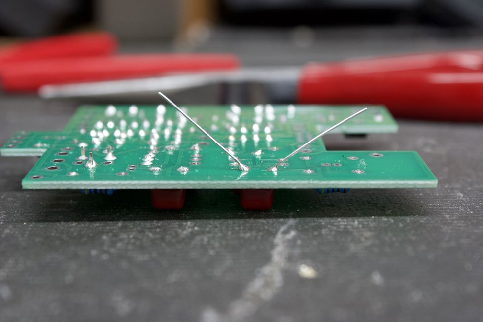
Photo 19
Step 10: Soldering Electrolytic Caps (page 15)
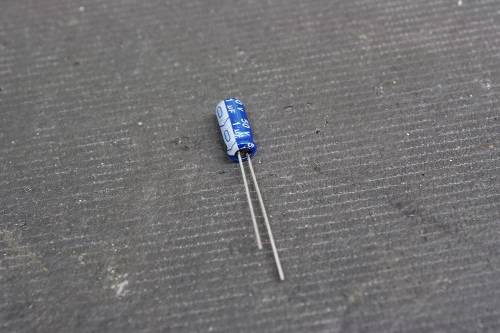
Photo 20
Let’s do the same thing here as we just did in Step 9. One thing to note is that electrolytic capacitors are polarized and need to be populated in the correct orientation. This is denoted on both the PCB and the component itself. On the PCB, the positive pad is denoted by the square pad. On the electrolytic capacitor, the positive lead is the longer leg. Additionally, the negative lead of the cap also corresponds to the white strip on the body (Photo 20).
So, let’s go ahead and populate the caps and solder them with either the foam trick or by bending the leads. Flush-cut the excess lead and we’re done (Photo 21).
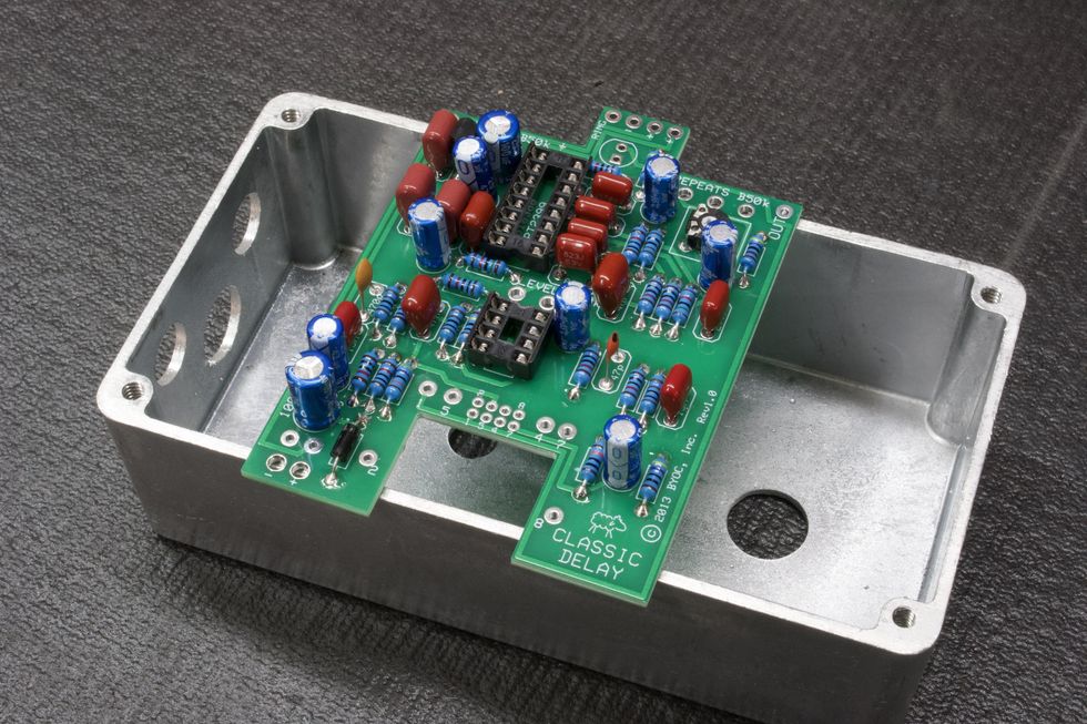
Photo 21
Step 11: Battery Snap and Hook-Up Wire
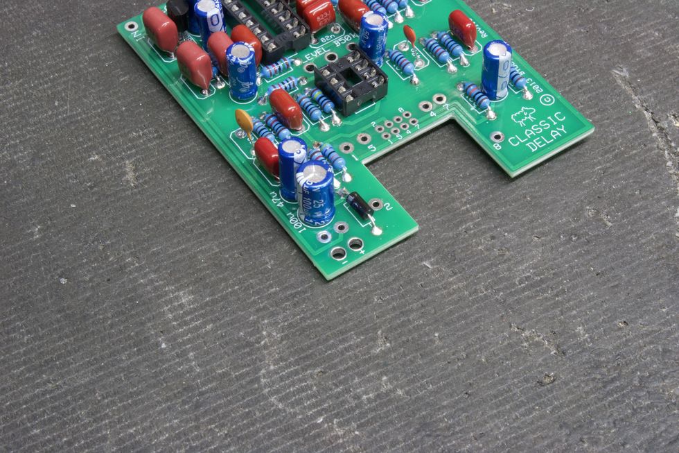
Photo 22
This DIY kit offers a battery option for those that feel so inclined. (See page 17 of the instructions.) For this step, we’ll need to connect the battery snap to the PCB. Before soldering, we’ll want to first feed the two wires through the holes directly below the solder pads. These holes act as strain relief for the battery snap and have + and - signs next to them (Photo 22). Then, simply solder the red wire to the positive (+) pad and the black wire to the negative (-) pad (Photo 23).
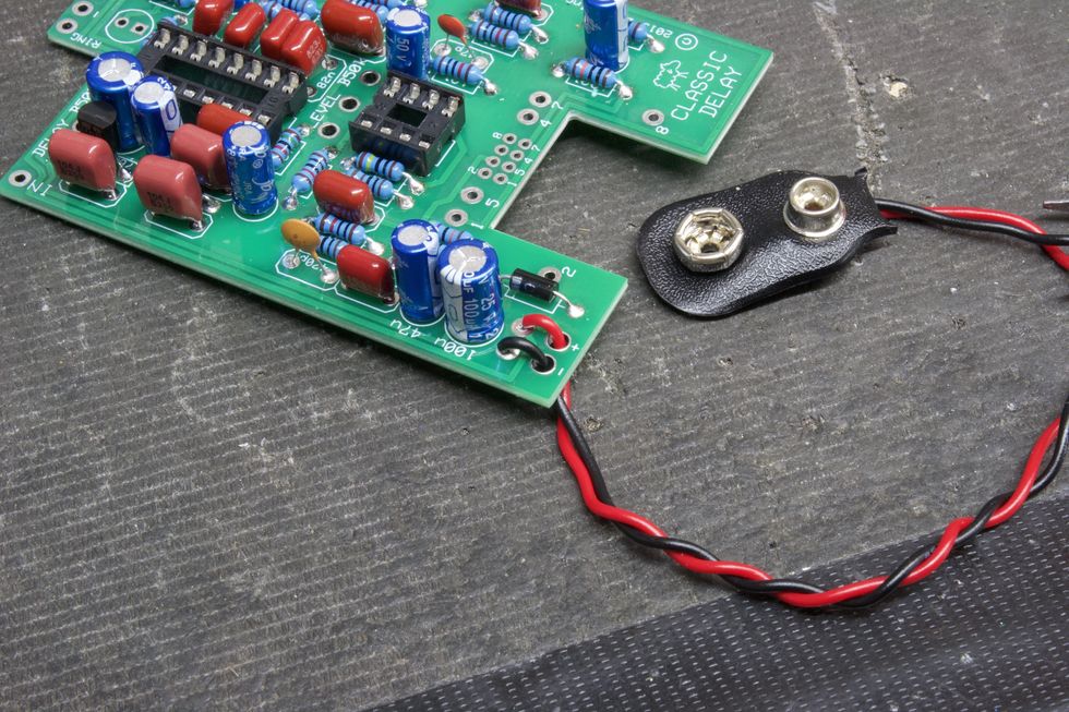
Photo 23
Next, we need to cut and strip the included wire (page 18). We need four 2.5" pieces of wire, and one 1.5" piece (Photo 24).
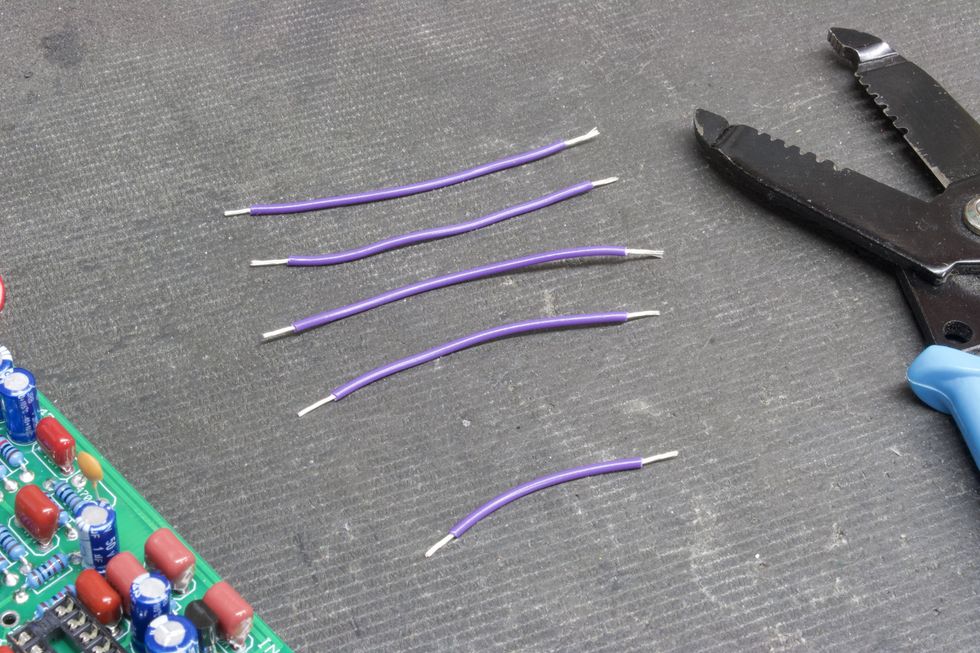
Photo 24
Place the 2.5" wires into the top side of the solder pads for in, out, and the two courtesy grounds—all handily marked. Then, solder from the bottom side. Do the same for the 1.5" wire going to the ring pad (Photo 25).
Tip: If painting the enclosure is desired, this is the last chance you’ll have to do it. After this, there will be components mounted to the chassis.
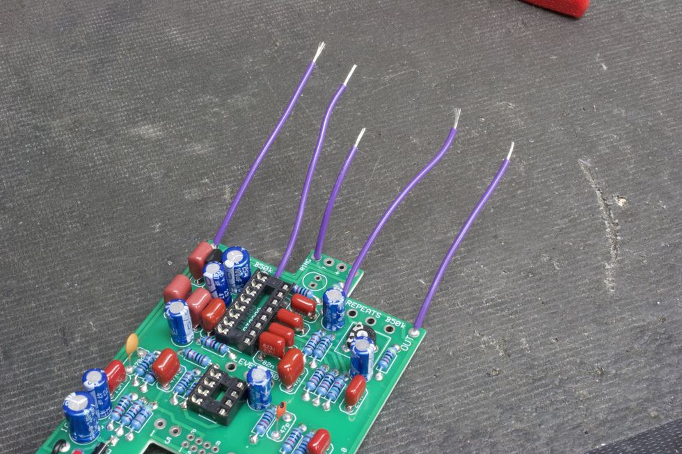
Photo 25
Step 12: Install DC Jack (page 19)
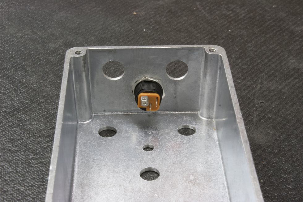
Photo 26
Place the DC jack into the large hole on the back heel of the enclosure and tighten the nut using a 14 mm (9/16") wrench (Photo 26).
Step 13: Potentiometers and Status LED (pages 20 and 21)
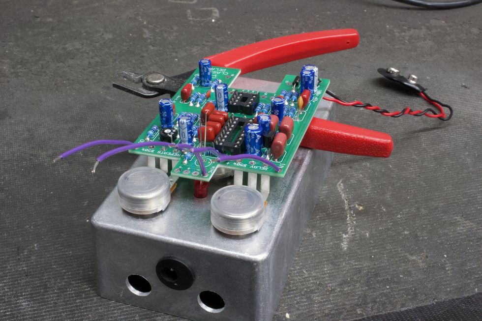
Photo 27
The included instructions for this next part have you mate the PCB to the inside of the enclosure. This will help line up the pots and LED. However, afterwards it will make soldering the remaining wire more difficult. Here’s a trick we can do that gives us the benefits of using the enclosure to help with pot alignment without needing to take the PCB out afterwards to solder the remaining wires. What we’ll want to do is simply use the face of the enclosure to hold the pots and set the LED height. Additionally, we can use the flush cutters to help balance the PCB (Photo 27). Be sure to have the long lead of the LED mate with the square pad, then solder away!
Step 14: Final Hook-Up Wire
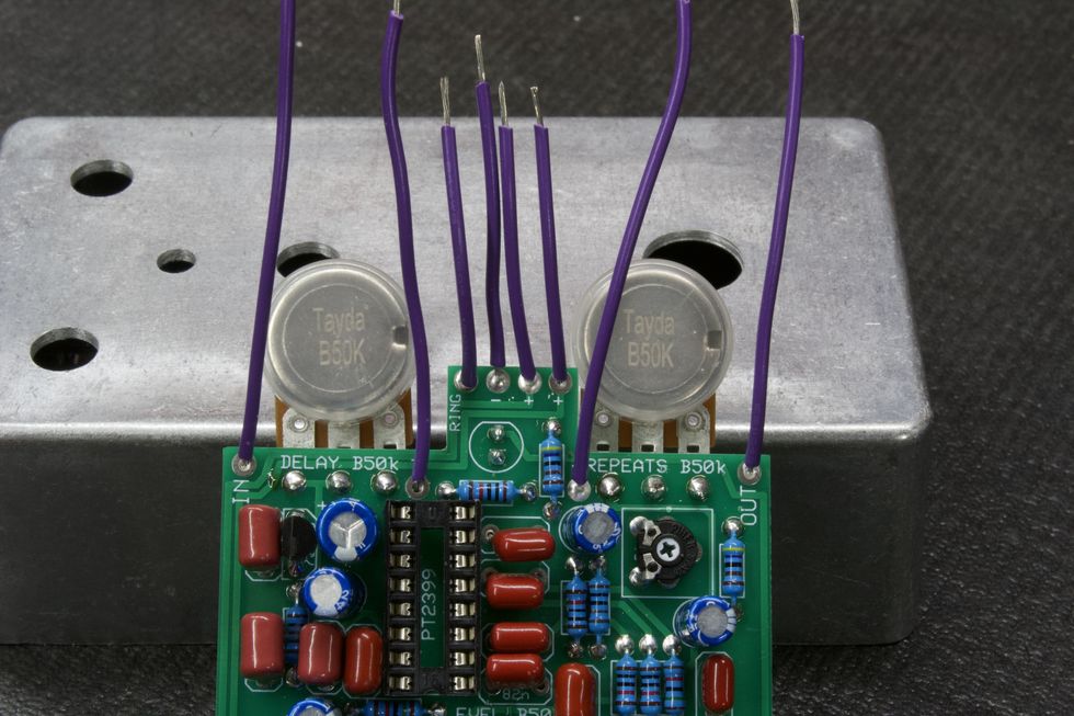
Photo 28
My steps continue to vary slightly from the instructions throughout the rest of the build, so you might want to do a side-by-side comparison. Let’s finish the wire for the DC jack next. Cut and strip three 1.5" pieces. These need to be placed into the three power pads at the top of the PCB marked -, +, + , as in Photo 28.
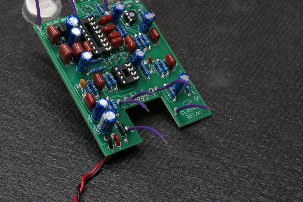
Photo 29
Next, cut and strip five more 1.5" pieces. Place these in the footswitch pads at the bottom of the PCB marked 1, 2, 5, 7, 8 as shown in Photo 29.
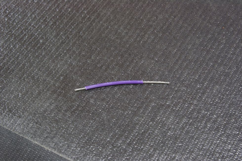
Photo 30
Last wire! Cut one 1.5" piece. Only for this one, strip half an inch off of one side (Photo 30). Place the short-stripped side into the footswitch pad labeled 4.
Step 15: Footswitch prep
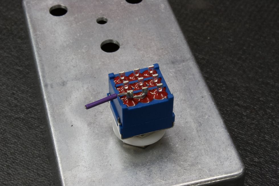
Photo 31
For the footswitch, we need to jump lugs 3 and 6. To do this, we’ll use the remaining wire. Place the footswitch into the correct hole on the face of the enclosure. Then, cut a 1" piece of wire and strip half of it. Feed the exposed wire through lug 3 and into lug 6 and then solder both (Photo 31). Cut the excess wire.
Step 16: Insert the IC
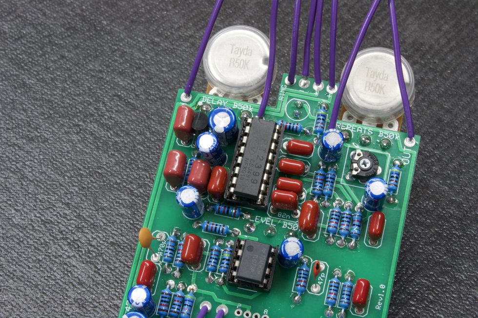
Photo 32
Now, we’re ready to insert the integrated circuits into their respective sockets. These need to be placed in the correct way, and there are two ways to identify them. Pin 1 is the top left leg of the IC—which is the rectangular black object in Photo 32. These legs are marked with a small dot in the top left corner or the upside of the IC is marked with a debossed half circle.
Step 17: Mounting and Final Soldering
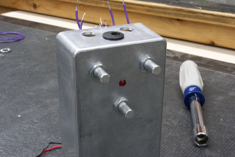
Photo 33
PCB: Now for the real fun! We’re ready to start inserting chassis-mounted components. Let’s start with the populated PCB. Place the PCB with the three pots lining up with the drilled holes, place the pot washers on the shafts, and then tighten the pot nuts using a 10 mm (25/64") nut driver/wrench, for the results in Photo 33.
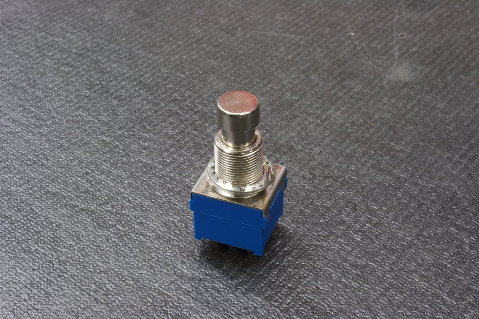
Photo 34
Footswitch: Now that the PCB is securely tightened, let’s go ahead and do the same for the footswitch. Remove all hardware from the footswitch bushing except for one nut and the lock washer (Photo 34).
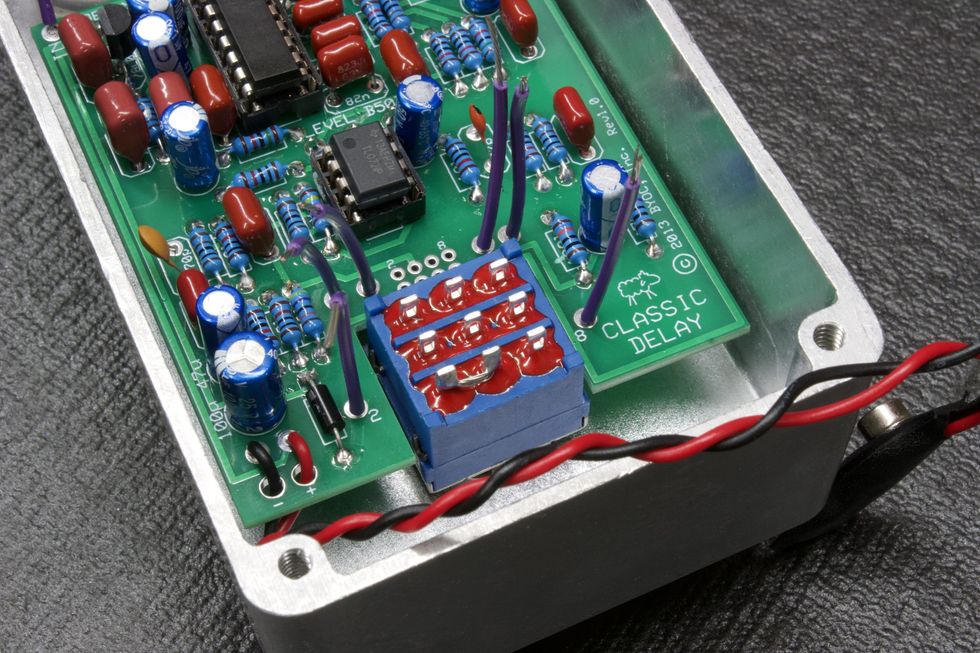
Photo 35
Feed the footswitch through the footswitch hole, making sure that the footswitch has the two poles that we soldered together facing the bottom left (Photo 35).
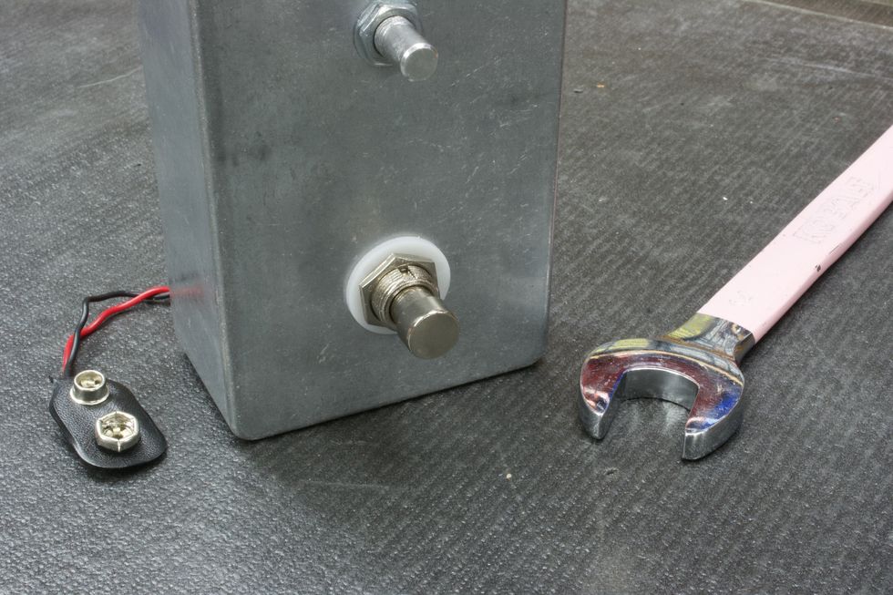
Photo 36
Next, place the plastic washer onto the bushing (optional), and tighten the hex nut with a 14 mm (9/16") wrench (Photo 36).
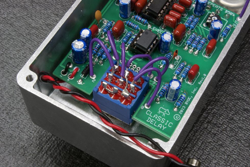
Photo 37
Lets go ahead and solder the footswitch wires to their respective footswitch poles (Photo 37). See the instructions’ page 26 for pole-numbering reference.
Tip: Solder from the top row down—i.e. 1, 4, 7, then 2, 5, 8.
Another tip: Remember that the wire for pole 4 also connects to pole 9.Step 18: DC Jack
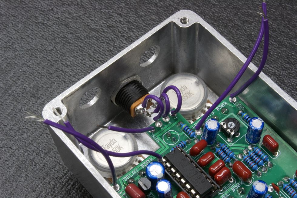
Photo 38
Next, we’ll need to solder the three wires that go to the DC jack, as explained in page 22 of the instructions. Start with the middle wire, since it sits the lowest and will be easier to get at without the other two wires in the way (Photo 38).
Step 19: Audio Jacks
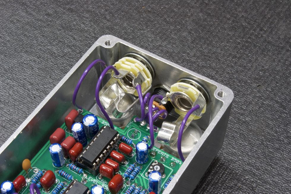
Photo 39
The last chassis-mounted components are the two audio jacks. Let’s do the stereo input jack first. Go to page 24 of the instructions to see how these jacks are oriented. The lock washer goes on the bushing first, then gets placed into the hole to the left of the DC jack. Then, place the washer onto the bushing and tighten the hex nut with a 1/2" nut driver/wrench.
Follow the same steps for the mono output jack. And then, it’s the final soldering step: Solder the wires to the appropriate lugs on the audio jacks (Photo 39), as on instructions page 28. Then, finally, place the knobs on, tighten them down, and we’re done!