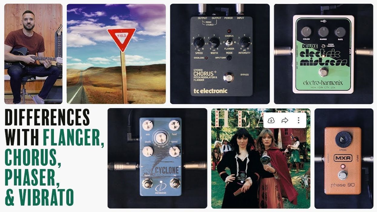
youtu.beDIY DIY: Chorus, Phaser, Flanger & Vibrato - Know the Differences! Nikos ArvanitisMar 11, 2024
Recording Dojo Stacking Effects? Keep a Beginner’s Mind Try breaking the signal-chain rules to create new—and dazzlingly retro—sounds for your recordings.Bryan ClarkMay 06, 2022
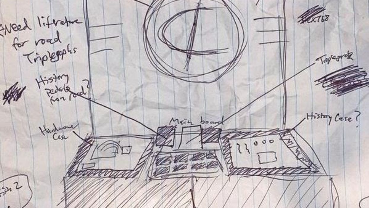
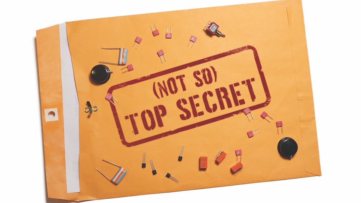
State of the Stomp Your Trade Secrets/Trade Your Secrets In the pedal-building community—as in Alcatraz—sharing is caring.Alex GuaraldiApr 19, 2022
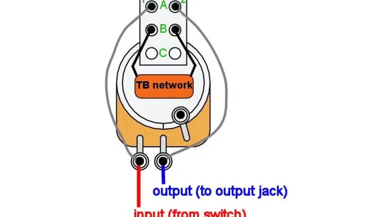
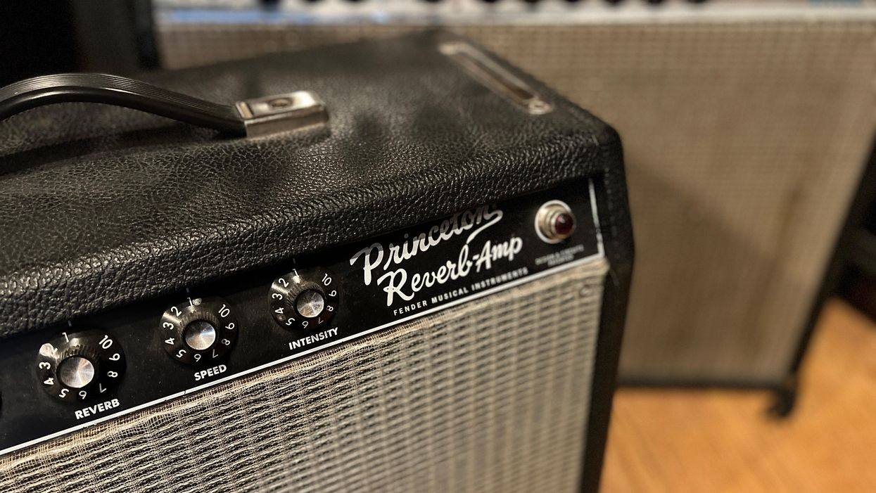
State of the Stomp Trimmer Adjustments Can Twist Funky Pedals Back into Shape Aisha Loe explains how to cure mushy modulation with a screwdriver—but you need to know what you’re doing.Aisha LoeApr 04, 2022
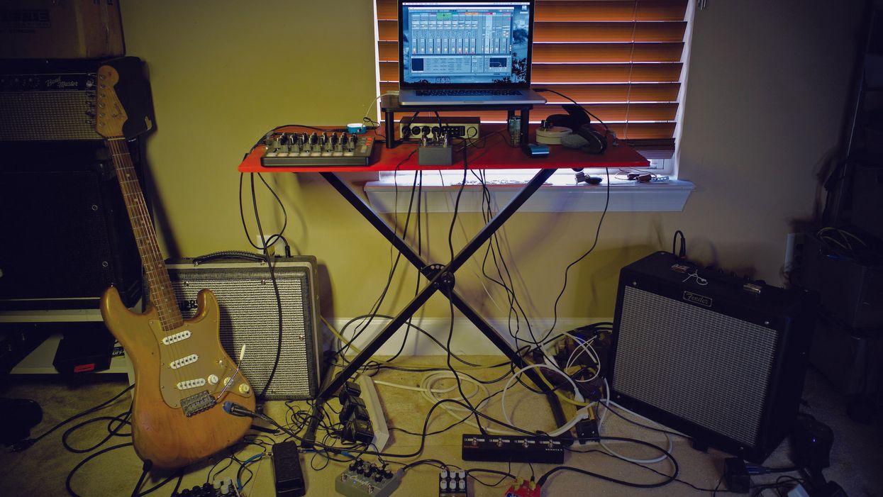
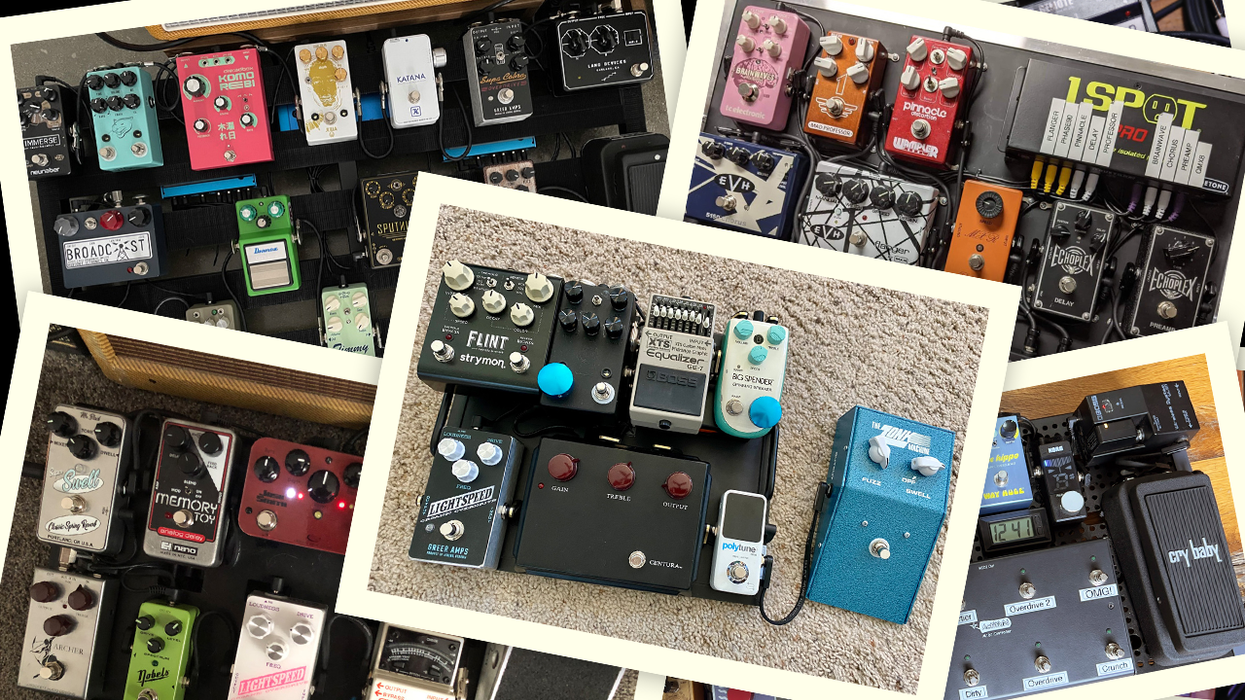
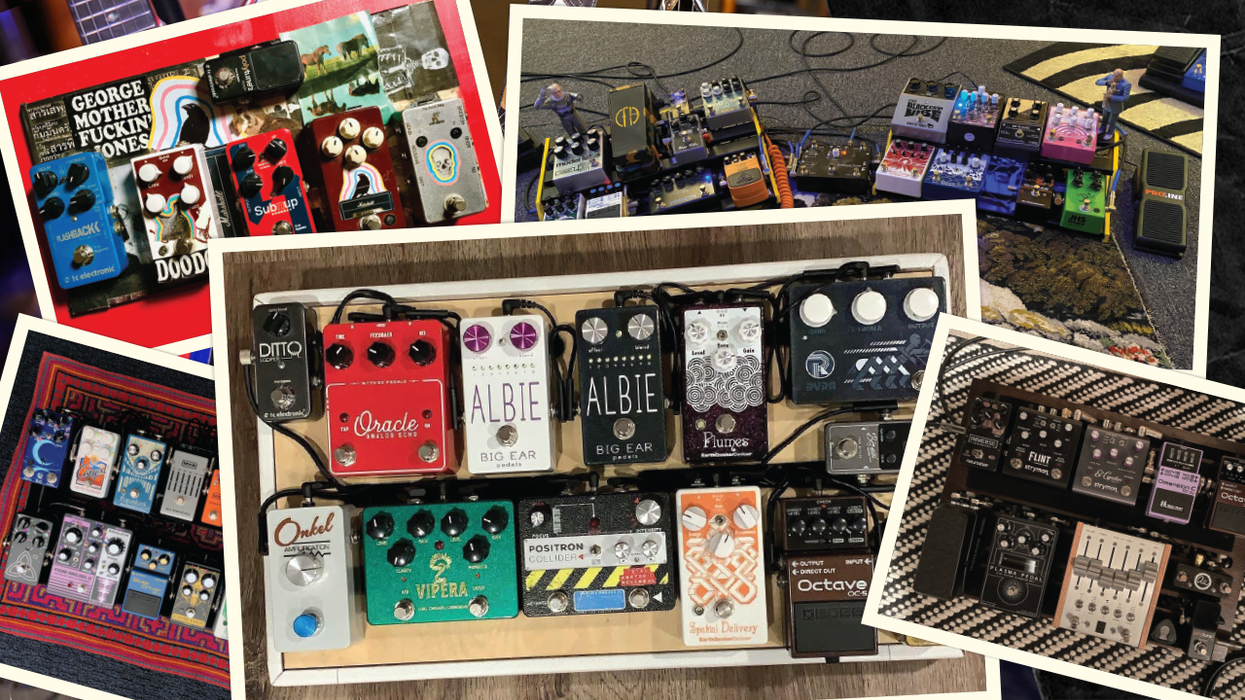
Gear Galleries Reader Pedalboards 2022, Pt. 2 Here we go again! Last month we brought you part one of your guitar cohorts’ boards from around the world. Time to dig in for part two.Premier GuitarMar 15, 2022
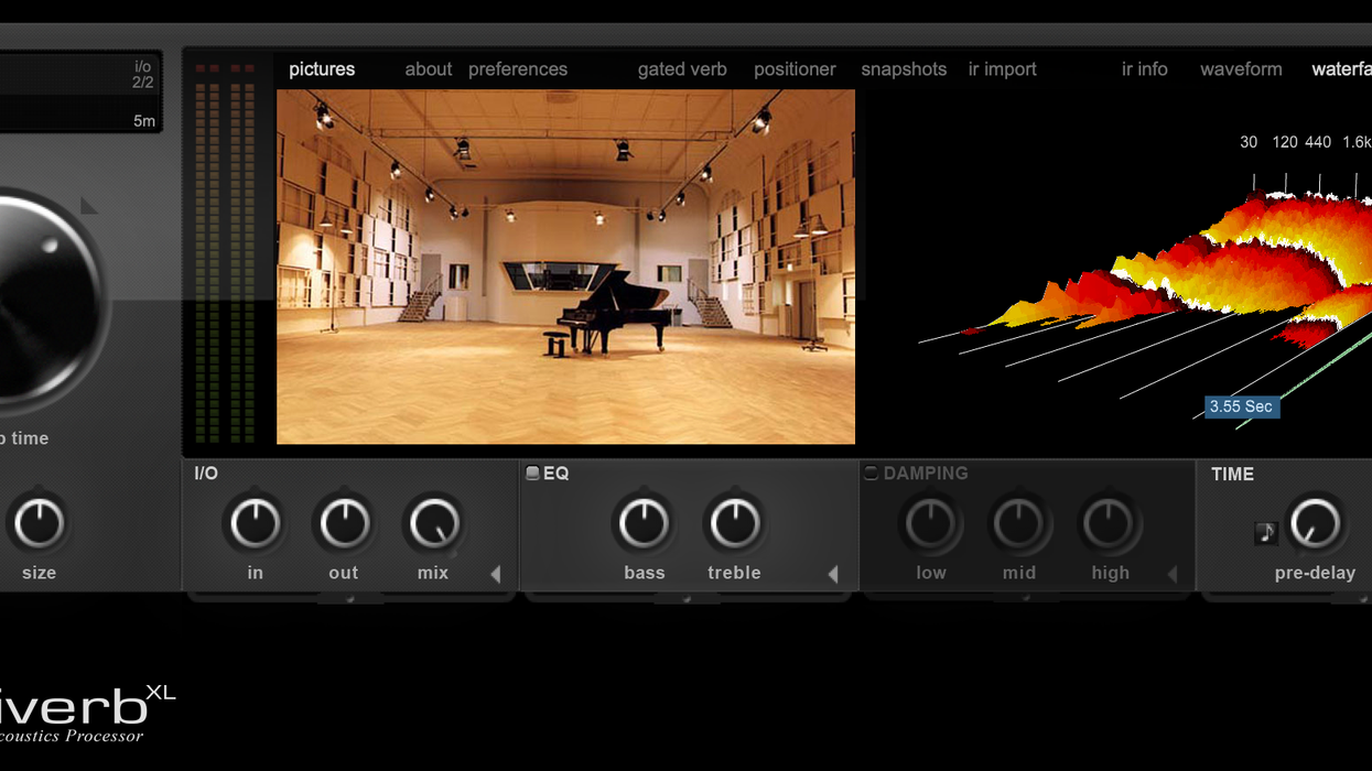
Recording Tips A Guitarist’s Guide to Reverb Plug-Ins The entire world of ’verb—from traditional to extreme—really does lie at your fingertips. Here’s how to access it.Joe GoreMar 14, 2022
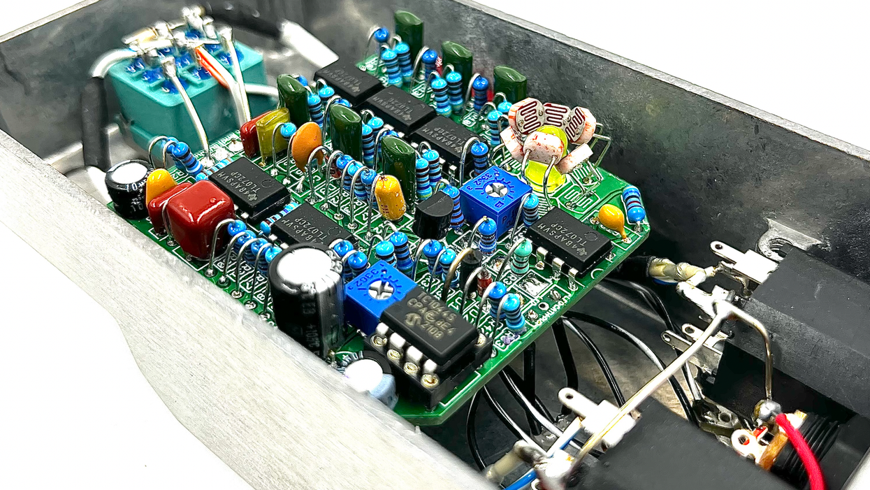
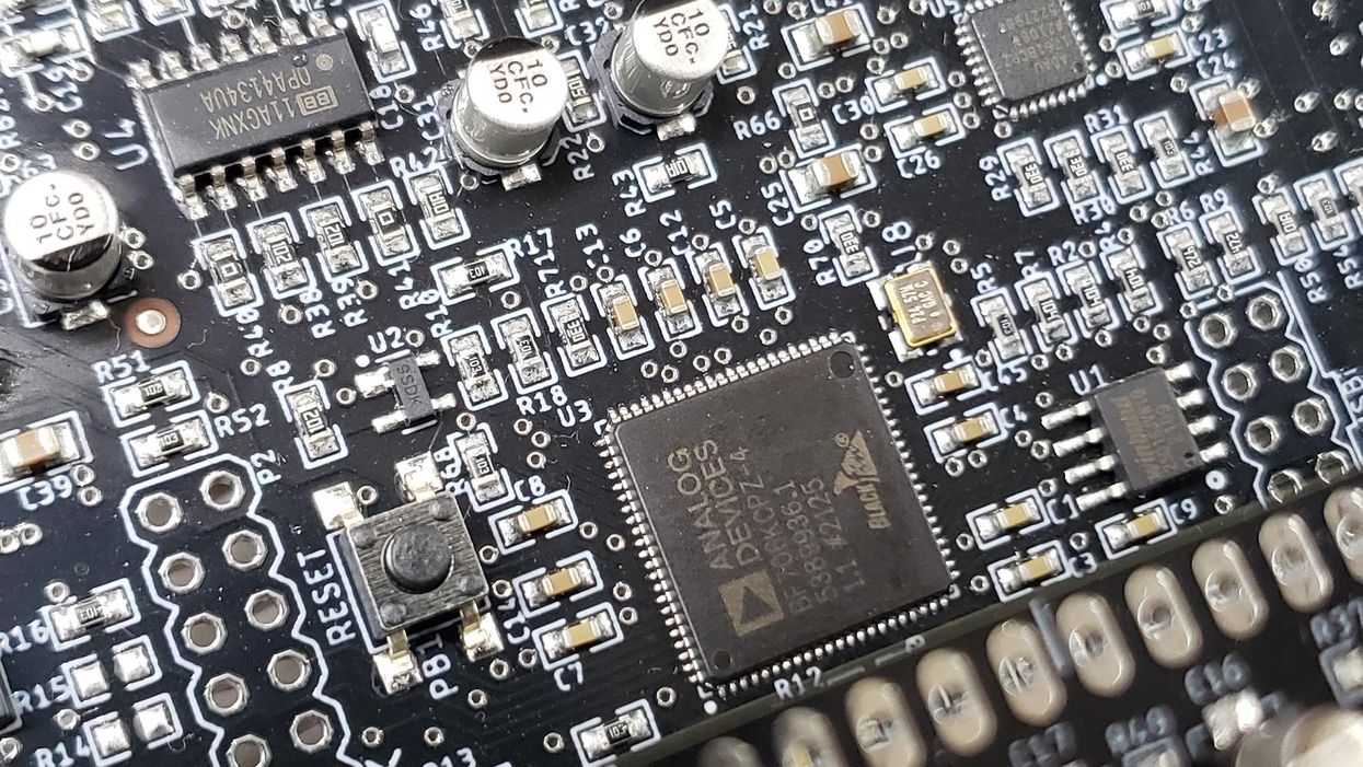
State of the Stomp What DIY-ers Need to Know About Pedal-Component Tolerances Yes, there's a lot of value variance, but there's an upside, too.Barry O’NealMar 14, 2022
State of the Stomp How Will Supply-Chain Issues Affect the Future of Pedal Building? CopperSound Pedals founder Alex Guaraldi's debut "State of the Stomp" outing looks at how compounding Covid woes are making life trickier for stompbox manufacturers.Alex GuaraldiFeb 09, 2022
Pedal Projects Reader Pedalboards 2022, Pt. 1 These days, there’s more time to spend in the pedal vortex. Behold the boards of fellow guitarists from around the world. Premier Guitar StaffFeb 08, 2022
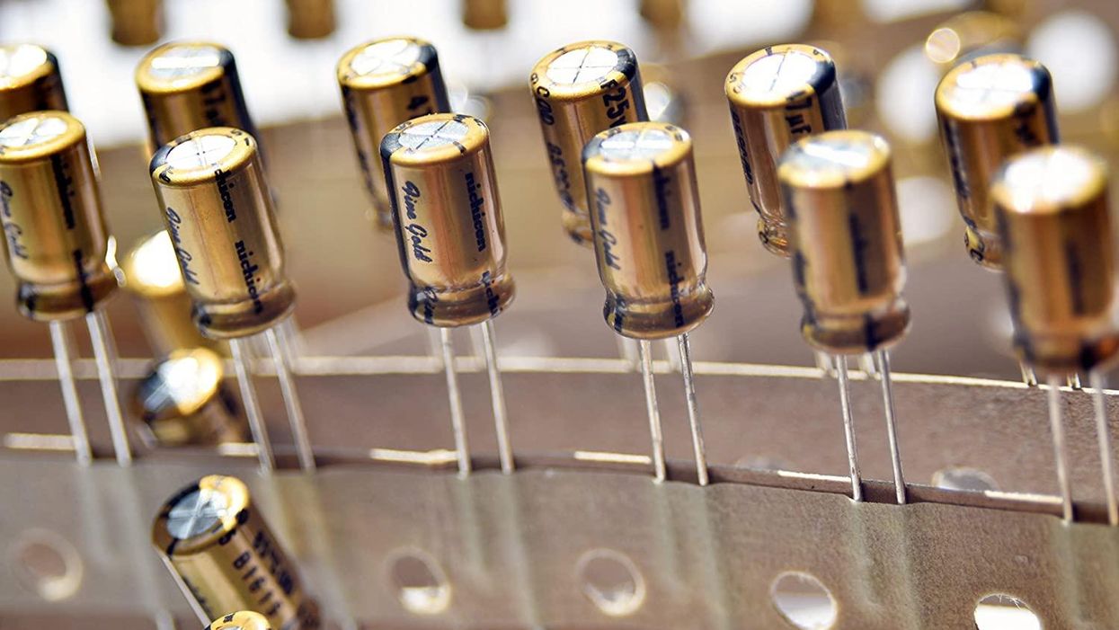
State of the Stomp Why New Caps Can Bring Old Pedals to Life Electrolytic capacitors are your stomps' first line of defense against bad current. Keep them healthy and your tones will be, too.Aisha LoeJan 03, 2022